Capability:Blind/Buried Via
Vias, that is, copper plated holes, play a key role in the interconnection between layers in a printed circuit board. Generally speaking, vias in PCBs can be classified into the following categories: through-hole via, blind via and buried via. Blind/buried vias are widely applied in SMT (Surface Mount Technology) just to compensate for disadvantages of through-hole vias.

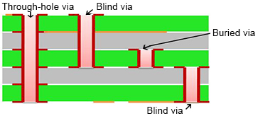
Blind via connects one external layer and one or more inner layers in printed circuit board, responsible for interconnection between top layer and inner layers or bottom layer and inner layers.
Buried vias connect only inner layers inside printed circuit board so that they are invisible just from the outer appearance of a PCB since they are internally “buried”.
Blind/buried vias conform to the density improvement of boards without the need to increase number of layers or board size. Therefore, blind/buried vias are usually applied in HDI PCBs. Put in another way, blind/buried vias can be picked up when you suffer from tight requirement of limited space and through-hole hassles.
Winco-PCB would help you manufacturer the Blind Via per IPC standard. Any question need to confirm with us, please send email to : [email protected] and our engineer would give you a fast answer.